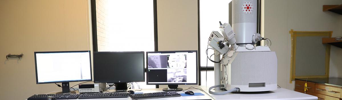
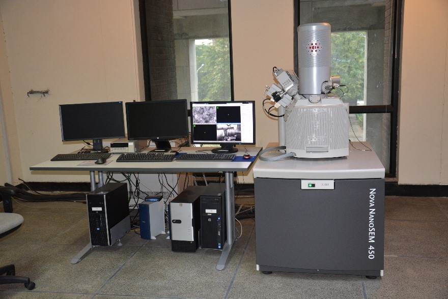
FEI Nova 450 NanoSEM
SEM is used to study topography, morphology and local chemical and phase composition from nanometers to millimeters. The Nova NanoSEM 450 field-emission scanning electron microscope (FE-SEM) delivers best-in-class imaging and analytical performance in a single, easy-to-use instrument and enables you to gain the most comprehensive answers in the least amount of time. This propels productivity without sacrificing the quality imaging you demand from your research work. With Nova NanoSEM you can easily switch instrument conditions based on types of samples you are investigating or types of analytical work you need to perform.

Download Rate List
Capabilities
- Surface sensitivity is delivered without sacrificing the resolution - Characterize a wide range of samples with unique low vacuum capabilities and ultra-high resolution low voltage imaging; low voltage [1kV] resolution is 1.4 nm in high vacuum mode, while for non-conductive materials, the Nova NanoSEM is unique in offering the highest resolution (1.8nm) at low voltages (3kV). The ultimate resolution is ~1 nm under ideal operating conditions.
- Delivered in one configuration: both a high-current beam, which is essential for rapid analytical research, and high resolution at high- and low-voltage, which is essential for image quality across a wide range of sample types.
- Strong performance in low vacuum mode gives you more analytical power - when you need top quality analytical data on samples like glass, ceramics or other non-conductive materials
- Analyze big, bulky samples with a large stage travel and large motorized Z travel.
- In-situ plasma cleaner reduces hydrocarbon contamination in the chamber and reduces the amount of carbon that is deposited on samples.
Standard Detectors
- Everhart-Thornley Detector (ETD)
- Through Lens Detector (TLD)
Advanced (External) Detectors
- Concentric Backscattered Detector (CBS)
- Scanning Transmission Electron Detector (STEM)
- Low Vacuum Detector (LVD)
Added Capabilities
- Energy Dispersive X-ray Spectroscopy
- E-beam Lithography
Request Form (for LUMS students / faculty)
Click here for SEM request form (for internal students only)
Contact
Dr. Murtaza Saleem, Senior Research Scientist | murtaza.saleem@lums.edu.pk
Associated Faculty
 |
 |
 |
| Dr. Salman N. Arshad salman.arshad@lums.edu.pk |
Dr. Sabieh Anwar sabieh@lums.edu.pk |
Dr. Irshad Hussain ihussain@lums.edu.pk |